 open the dielectric materials definition window
Dielectric Materials
open the dielectric materials definition window
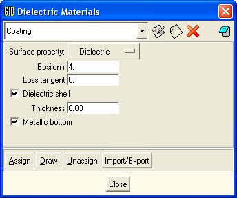
The default material for the whole geometry is a perfect conductor (metal). However, it is possible to assign dielectric properties to surfaces. There are 2 ways to define a dielectric material :
In the case of a dielectric layer, the relative permittivity (εr and loss tangent) is required. If the layer is not infinite, the Dielectric shell button must be checked. In that case, the thickness of the layer is required. In addition, the finite layer may have a metallic bottom.
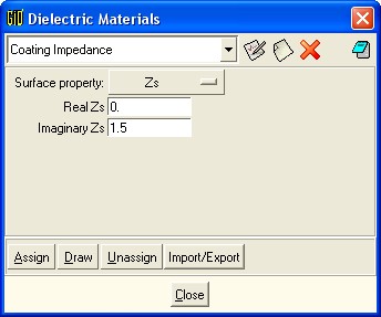
A surface impedance is simply given by its real part and its imaginary part. The normalized surface impedance is required. In other words, the actual surface impedance must be divided by the vacuum impedance (about 377 ohms). The following example is equivalent to the previous one, if the frequency is 1 GHz. In the case of a thin coating over a metallic surface, the surface impedance (not normalized) is given by :
![]()
where j=sqrt(-1), ω=2π*frequency and d is the thickness of the coating.
There are basic materials in the initial list. They contain approximate values. In addition, these values may be frequency dependent. It is possible to add new materials with the function new dielectric material . The new material will be only saved in the current project. Similarly, the modification of existing material will be saved only in the current project. It is also possible to import the materials from other projects with the function Import/Export. If this function is applied to the IDRA.mat file (default file for new projects) in the IDRA.gid project, it can also export the new materials to the default list.
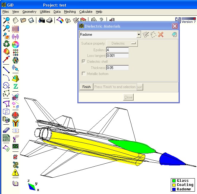
The Draw utility gives an easy graphical check of the assigned materials :
Copyright © 2009, IEEA